
Information contained in this news release is current as of the date of the press announcement, but may be subject to change without prior notice.
New DRAM circuit design approach for gigabit-era DRAM (PDF Type, 16 kByte)![]()
February 10, 2005
New DRAM circuit design approach for gigabit-era DRAM
Achieved industry’s first integration of a calibration system in PLL and a +/-2% calibration accuracy
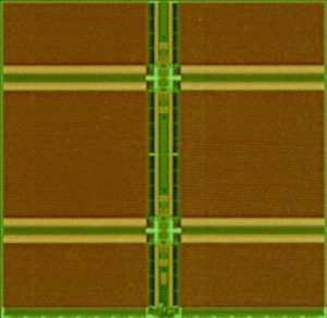
90nm on-chip SRAM module (work memory)
Tokyo, 10th February 2005 — Hitachi, Ltd. (NYSE:HIT / TSE: 6501) and Renesas Technology Corp. announced that they have developed low-voltage embedded SRAM technology for SoC’s (system-on-a-chip) beyond the 90-nm process node. Using new circuit techniques, the power lines of SRAM cells were placed in a “floating state” (detached from the power supply) during write operations, and 0.8V operation was confirmed. This development will help overcome the barrier to maintaining low-voltage operation which is becoming increasingly more difficult to achieve due to process scaling, and is expected to become fundamental technology for achieving both high-performance and low-power operation in SoCs embedded in information devices, which are supporting the growth of the ubiquitous society.
In SoC’s, which processes multimedia files in information devices such as cellular phones, “high-speed” and “low-power” are essential features. Conventionally, high-speed performance was achieved by transistor scaling and low-power operation by supply-voltage scaling. Beyond the 90-nm process node, however, the effect of performance variations in the transistors can no longer be ignored and achieving higher performance through conventional methods is becoming difficult. This is especially so for SRAM circuits. As the amount of data that a SoC needs to process increases, SRAM capacity must also increase, and thus even a small performance variation between transistors has a large effect on performance, making it difficult to further lower the supply voltage. Thus the supply voltage for the SRAM circuit is expected to create a limit on the degree to which low-power operation can be achieved in SoC’s, and the development of new low-voltage technology for SRAM in the 90nm process node and beyond, is a considered critical issue for achieving low-power SoC’s.
In response to this challenge, Hitachi and Renesas Technology have developed the low-voltage and low-power technology for embedded SRAM in SoC’s beyond 90-nm process node. Features of the technology are as below:
- Power-line floating write techniques for low-voltage operation: The power line of SRAM for retaining data is placed in a floating state (detached from the power supply) during a write operation, creating a condition where it is easier to re-write the data in the memory cell. This enables the write operation to be conducted with low supply voltage, and at the same time lowering the operating voltage of the entire SRAM.
- Write replica circuit for low-power write operation: Conventionally, during the entire time assigned to a write operation, all the write circuits are activated in order to attain good write performance. This new technique monitors the write performance using a replica circuit, and the write-circuit activating time is changed according to the write performance. This enables unnecessary power consumption to be reduced without performance degradation.
Hitachi and Renesas have fabricated prototype chips with 32-kbit SRAM module for cache memory(*1) and 512-kbit SRAM module for working memory,(*2) and evaluated its performance. Compared to the conventional SRAM modules, the supply voltage is 100-mV lowered and the SRAM modules can operate at 0.8-V supply voltage. The write replica circuit reduces its power consumption by 18%, and achieves the power performance, 0.76 µW/MHz bit.
The circuit technology developed is expected to contribute significantly to overcoming a scaling barrier to achieving low-power and low-voltage operation in embedded SRAM beyond the 90nm process node.
These results were presented at the IEEE International Solid-State Circuits Conference (ISSCC 2005), held in San Francisco, California, U.S.A., from 6th February 2005.
Technical Terms:
(*1) Cache memory: High-speed memory in a CPU. It retains frequently used data and contributes to the high-performance of the CPU.
(*2) Working memory: High-capacity memory which retains the data used by a user.
About Elpida Memory, Inc.
Elpida Memory, Inc. is a manufacturer of Dynamic Random Access Memory (DRAM) silicon chips with headquarters based in Tokyo, Japan, and sales and marketing operations located in Japan, North America, Europe and Asia. Elpida’s state-of-the-art semiconductor wafer manufacturing facility is located in Hiroshima, Japan. Elpida offers a broad range of leading-edge DRAM products for high-end servers, mobile phones, digital television sets and digital cameras as well as personal computers. Elpida had sales of 100.4 billion yen during the fiscal year ending March 31, 2004. For more information on Elpida, please visit the company’s Web site at http://www.elpida.com.